- 您现在的位置:买卖IC网 > Sheet目录508 > SI3445DV-T1-GE3 (Vishay Siliconix)MOSFET P-CH 8V 6-TSOP
Si3445DV
Vishay Siliconix
P-Channel 1.8-V (G-S) MOSFET
PRODUCT SUMMARY
FEATURES
V DS (V)
-8
R DS(on) ( Ω )
0.042 at V GS = - 4.5 V
0.060 at V GS = - 2.5 V
0.080 at V GS = - 1.8 V
I D (A)
± 5.6
± 4.7
± 2.9
? Halogen-free According to IEC 61249-2-21
Definition
? TrenchFET ? Power MOSFETs
? 1.8 V Rated
? Compliant to RoHS Directive 2002/95/EC
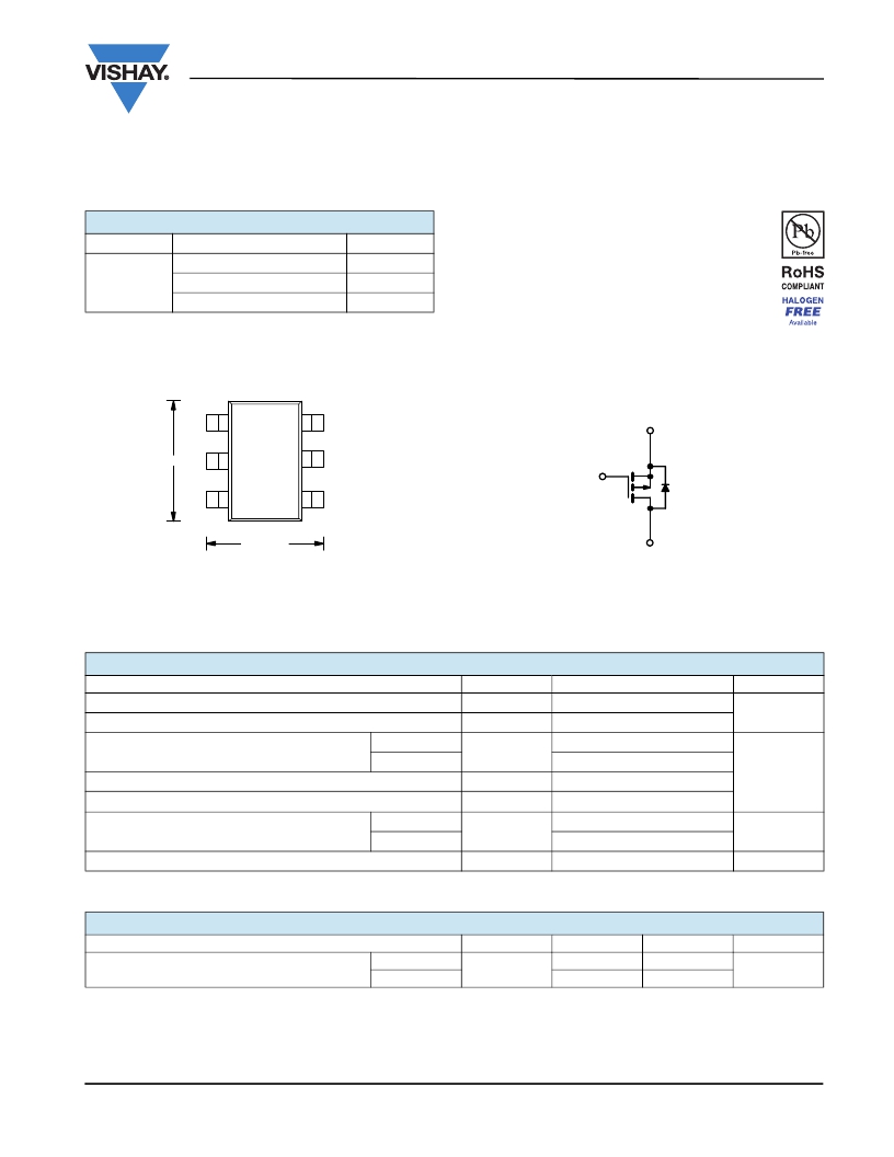
TSOP-6
Top V ie w
1
6
(4) S
3 mm
2
3
5
4
(3) G
2.85 mm
(1, 2, 5, 6) D
Orderin g Information: Si3445D V -T1-E3 (Lead (P b )-free)
Si3445D V -T1-GE3 (Lead (P b )-free and Halogen-free)
ABSOLUTE MAXIMUM RATINGS T A = 25 °C, unless otherwise noted
P-Channel MOSFET
Parameter
Drain-Source Voltage
Gate-Source Voltage
Symbol
V DS
V GS
Limit
-8
±8
Unit
V
Continuous Drain Current (T J = 150 °C) a, b
Pulsed Drain Current
Continuous Source Current (Diode Conduction) a, b
Maximum Power Dissipation a, b
Operating Junction and Storage Temperature Range
T A = 25 °C
T A = 70 °C
T A = 25 °C
T A = 70 °C
I D
I DM
I S
P D
T J , T stg
± 5.6
± 4.5
± 20
- 1.7
2.0
1.3
- 55 to 150
A
W
°C
THERMAL RESISTANCE RATINGS
Parameter
Symbol
Typical
Maximum
Unit
Maximum Junction-to-Ambient a
t ≤ 5s
Steady State
R thJA
106
62.5
°C/W
Notes:
a. Surface Mounted on FR4 board.
b. t ≤ 5 s.
Document Number: 70820
S09-0766-Rev. C, 04-May-09
www.vishay.com
1
发布紧急采购,3分钟左右您将得到回复。
相关PDF资料
SI3454ADV-T1-GE3
MOSFET N-CH 30V 3.4A 6TSOP
SI3455ADV-T1-GE3
MOSFET P-CH 30V 2.7A 6TSOP
SI3457BDV-T1-GE3
MOSFET P-CH 30V 3.7A 6-TSOP
SI3457DV
MOSFET P-CH 30V 4A SSOT-6
SI3458BDV-T1-GE3
MOSFET N-CH 60V 4.1A 6-TSOP
SI3460BDV-T1-GE3
MOSFET N-CH 20V 8A 6-TSOP
SI3460DV-T1-E3
MOSFET N-CH 20V 5.1A 6TSOP
SI3464DV-T1-GE3
MOSFET N-CH D-S 20V 6-TSOP
相关代理商/技术参数
SI3446ADV
制造商:VISHAY 制造商全称:Vishay Siliconix 功能描述:N-Channel 20-V (D-S) MOSFET
SI3446ADV-T1-E3
功能描述:MOSFET 20V 6.0A 3.2W RoHS:否 制造商:STMicroelectronics 晶体管极性:N-Channel 汲极/源极击穿电压:650 V 闸/源击穿电压:25 V 漏极连续电流:130 A 电阻汲极/源极 RDS(导通):0.014 Ohms 配置:Single 最大工作温度: 安装风格:Through Hole 封装 / 箱体:Max247 封装:Tube
SI3446ADV-T1-GE3
功能描述:MOSFET 20V 6.0A 3.2W 37mohm @ 4.5V RoHS:否 制造商:STMicroelectronics 晶体管极性:N-Channel 汲极/源极击穿电压:650 V 闸/源击穿电压:25 V 漏极连续电流:130 A 电阻汲极/源极 RDS(导通):0.014 Ohms 配置:Single 最大工作温度: 安装风格:Through Hole 封装 / 箱体:Max247 封装:Tube
SI3446DV
功能描述:MOSFET SSOT6 SINGLE NCH RoHS:否 制造商:STMicroelectronics 晶体管极性:N-Channel 汲极/源极击穿电压:650 V 闸/源击穿电压:25 V 漏极连续电流:130 A 电阻汲极/源极 RDS(导通):0.014 Ohms 配置:Single 最大工作温度: 安装风格:Through Hole 封装 / 箱体:Max247 封装:Tube
SI3446DV-T1
功能描述:MOSFET 20V 5.3A 2W RoHS:否 制造商:STMicroelectronics 晶体管极性:N-Channel 汲极/源极击穿电压:650 V 闸/源击穿电压:25 V 漏极连续电流:130 A 电阻汲极/源极 RDS(导通):0.014 Ohms 配置:Single 最大工作温度: 安装风格:Through Hole 封装 / 箱体:Max247 封装:Tube
SI3446DV-T1-E3
功能描述:MOSFET 20V 5.3A 2W RoHS:否 制造商:STMicroelectronics 晶体管极性:N-Channel 汲极/源极击穿电压:650 V 闸/源击穿电压:25 V 漏极连续电流:130 A 电阻汲极/源极 RDS(导通):0.014 Ohms 配置:Single 最大工作温度: 安装风格:Through Hole 封装 / 箱体:Max247 封装:Tube
SI3446DV-T3
制造商:Vishay Semiconductors 功能描述:
SI3447
制造商:FAIRCHILD 制造商全称:Fairchild Semiconductor 功能描述:P-Channel 1.8V Specified PowerTrench MOSFET
